A closeup shot of an Intel die, with a pin for size reference.
In the semiconductor world, integration is omnipresent, driven by Moore’s Law. Integration reduces power and cost while increasing performance. The latest realization of this trend is the System-on-a-Chip (SoC) approach pervasive among PCs, tablets, and smartphones. And the latest SoC is Haswell.
Haswell is the first new family of SoCs from Intel to target the 22nm FinFET process, which uses a non-planar transistor that wraps around the gate on three sides. While Ivy Bridge was the first family of 22nm products, it was not fully optimized for the 22nm process. The CPU was a shrink of the 32nm Sandy Bridge rather than a new design.
The Haswell family encompasses a new CPU core, a new GPU, and numerous system-level changes. More importantly, it marks the beginning of Intel's more unified approach to SoCs. The Haswell family is really a set of building blocks that architects will assemble for specific markets. The Haswell CPU core is a step forward in performance (as is to be expected from Intel) but more importantly, it is a huge step down in power. This SoC should be viable for high-end tablets. Variants of Haswell are aimed as low as 10W, and future improvements may reduce this further. Intel’s 22nm FinFET node is necessary to achieve this wider range, but it's not sufficient. Haswell's architecture fully exploits the benefits of the new process technology in a way that Ivy Bridge never did. It ultimately yields higher performance and lower power, which will translate into PCs and tablets that run faster with a longer battery life.
At the instruction set level, the Haswell core supports four extensions that profoundly transform the x86 ISA. AVX2 widens integer SIMD (Single Instruction Multiple Data, a form of vectors) to 256-bit vectors, and that adds a gather instruction for irregular memory access. The fused multiply-add (FMA) instructions improve performance for floating point (FP) workloads. For cryptography, networking, and certain search operations, there are new bit manipulation instructions. Lastly, Haswell is the first widely available product with transaction memory through the TSX extension. TSX is an incredibly powerful model for multi-threaded programming that improves performance and efficiency of software by better utilizing the underlying multicore hardware. Microarchitecturally, the Haswell core achieves even higher performance than Sandy Bridge. The improvements are mainly in the out-of-order execution—especially the memory hierarchy. It all strengthens Haswell's case to be the basis of Intel's upcoming generation of products in everything from tablets to servers.
Haswell instruction set and front-end
Haswell introduces four families of new instructions. The first is AVX2, which is a 256-bit extension of existing integer SIMD. It's essentially the counterpart of the floating-point AVX instructions. AVX2 also adds vector permutes and shifts, then gathers, instructions for loading data from non-contiguous addresses. Gather is crucial for compilers to take advantage of wider SIMD instructions (e.g., AVX2 can have 32 byte long elements).
On the floating point side, Intel's new Fused Multiply Add (FMA) extension includes both 256-bit and 128-bit instructions. Compared to the conventional separate multiply and add instructions in SSE, FMA doubles the theoretical throughput. In addition, the fused instructions eliminate the intermediate rounding stage which can improve accuracy for some approximation algorithms.
The third extension is smaller and more focused on integer bit manipulation (known as BMI) for use in cryptography and packet handling. As an aside, Haswell adds a big-endian move instruction (MOVBE) that can convert to and from traditional x86 little-endian format (big-endian data stores the most significant byte first, while little endian stores the least significant byte first). This was originally introduced in Atom, and it was added to ensure full compatibility and improve performance for embedded applications.
The most significant ISA extension is TSX, which has been extensively discussed in a previous article on Haswell's transactional memory. In short, TSX separates performance from correctness for multi-threaded programs. Programmers can write simple code that is easier to debug, while the hardware extracts concurrency and performance.
Coarse-grained locking (e.g., locking an entire data structure) is easy to develop, especially when starting with single threaded code. However, fine-grained locking (e.g., locking a portion of the data structure such as a single node in a B-tree) is almost always higher performance. Hardware Lock Elision (HLE) uses hint prefixes to transparently provide the performance and throughput of fine-grained locking, even when programmers use coarse-grained locks.
Restricted Transactional Memory (RTM) is a new programming model that exposes explicit transactions through new instructions. These transactions can span complex data structures and be composed easily. However, it does require linking new libraries using RTM and possibly rewriting software to get the full benefits.
The new instruction set extensions are clearly the biggest change in Haswell's front-end. At a high level, instruction fetch and decode microarchitecture is largely similar to Sandy Bridge, but there are numerous subtle enhancements to note.
The branch prediction for Haswell has improved, although Intel was unwilling to share the specific details. The instruction cache is still 8-way associative, 32KB, and dynamically shared by the two threads. Likewise, the instruction TLBs are the same capacity. The major changes are enhancing instruction cache misses and prefetching to make better use of the existing resources. Instruction fetching from the instruction cache continues to be 16B per cycle, but with more outstanding L1 misses and more timely prefetching.
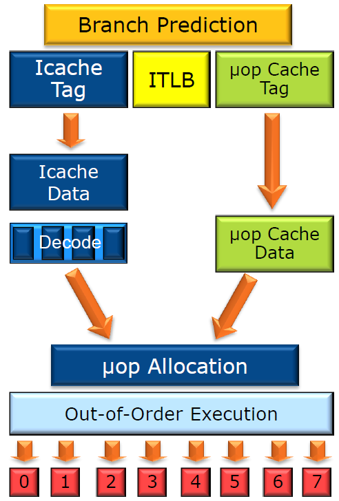
The decoding for Haswell is largely identical to Sandy Bridge. There are four legacy decoders that take in x86 instructions and emit simpler uops. The first is a complex one that can emit 1-4 fused uops and three simple decoders that can emit one fused uop each. Like Sandy Bridge, there is compare+jump fusion and stack pointer elimination. The Haswell uop cache is also identical, with 32 sets of eight cache lines. Each cache line holds up to six uops.
The Haswell uop queue was redesigned to improve single threaded performance. Sandy Bridge had two 28 entry uop queues, one for each thread. However, in Ivy Bridge the uop queues were combined into a single 56 entry structure. The chief advantage is that when a single thread is executing on Ivy Bridge or Haswell, the entire 56 entry uop buffer is available for loop caching and queuing.
Haswell out-of-order scheduling
Haswell is substantially wider than Sandy Bridge with more resources for dynamic scheduling, but it retains the same overall organization and function. Once decoded, uops are renamed and issued to the scheduler. In turn, the scheduler (sometimes called the reservation station) fans out to a number of ports containing execution units.
The first part of out-of-order execution is register renaming. The renamer will map architectural source and destination x86 registers used in the uops to the underlying physical registers. The renaming stage also allocates other bookkeeping resources, such as load, store, and branch buffer entries. Lastly, uops are bound to particular ports for downstream execution and sent to the scheduler to await execution.
The renamer can take four fused uops, allocate the appropriate resources, and rename registers to eliminate false dependencies. The renaming occurs for a single thread at a time, alternating as appropriate. These fused uops can be quite complex; for example, a fused load+execute uop might map to two actual uops, a load, and a dependent arithmetic operation.

Both Haswell and Sandy Bridge have unified resources for integer and vector instructions; these out-of-order resources are split evenly between two active threads. In contrast, AMD's Bulldozer and Jaguar separate the vector and integer pipelines.
The Haswell out-of-order window has grown modestly, along with an attendant increase in various other resources. The ROB holds status information about each uops and has grown from 192 entries. The ROB is statically split between two threads, giving each a window of 96 fused uops. Other structures are dynamically shared.
The integer register file is mostly used for scalar integer instructions, and it grew to 168 entries. AVX2 is a major feature in Haswell, and there are 24 additional registers for vector renaming. The number of loads and stores in-flight also increased, to a total of 72 loads and 42 stores.
The unified scheduler in Haswell is now 60 entries, up from 54 in Sandy Bridge. Those entries are dynamically shared between the active threads. Once ready, uops in the scheduler are sent to the execution units through dispatch ports. Haswell and Sandy Bridge both retire up to four fused uops/cyclein-order.
The new gather instructions in AVX2 are microcoded and map to multiple loads. This is not the most efficient implementation, and Broadwell and future architectures will improve the functionality over time. The gather instruction is still more efficient than an equivalent programmer construct. More importantly, it's easy for a compiler to emit.
The transactions introduced with TSX are fairly straightforward from a hardware standpoint. A transaction abort is handled similarly to a branch mispredict, and there is a limit of no more than seven nested transactions. (This may change in future implementations, however.)
Haswell execution units
The execution units in Haswell are tremendously improved over Sandy Bridge, particularly to support AVX2 and the new FMA. Haswell adds an integer dispatch port and a new memory port, bringing the execution to eight uops/cycle. But the biggest changes are to the vector execution units. On the integer SIMD side, the hardware has been extended to single cycle 256-bit execution. For floating point vectors, the big change is 256-bit fused multiply add units for two of the execution ports. As a result, the theoretical peak performance for Haswell is more than double that of Sandy Bridge.
Every cycle, up to eight uops are sent from the unified scheduler to the dispatch ports. As shown in Figure 3, computational uops are dispatched to ports 0, 1, 5, and 6 and executed on the associated execution units. The execution units include three types: integer, SIMD integer, and FP (both scalar and SIMD).
Port 6 on Haswell is a new scalar integer port. It only accesses the integer registers and handles standard ALU (Arithmetic Logic Unit) operations, including shifts and branches that were previously on port 5 (in Sandy Bridge). One of the advantages of the new integer port is that it can handle many instructions while the SIMD dispatch ports are fully utilized.
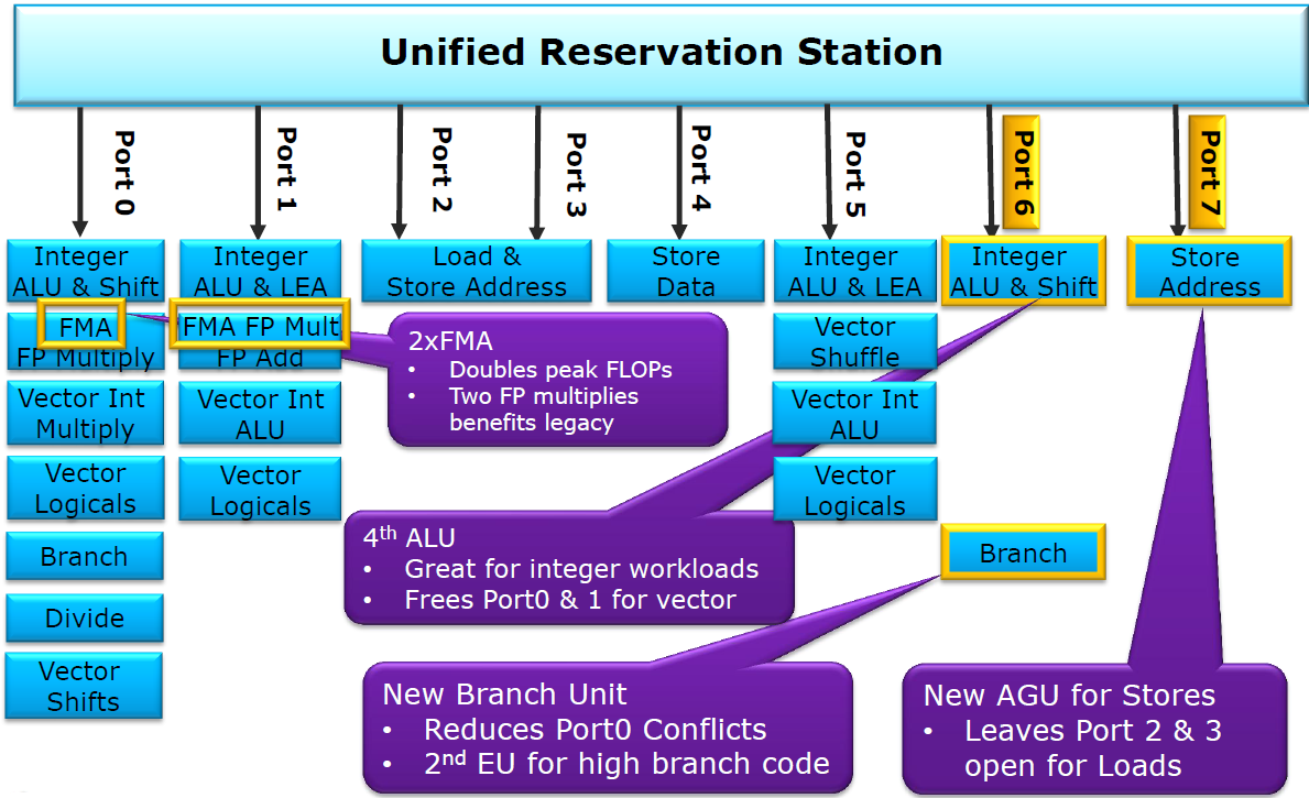
Turning to the SIMD execution units, Haswell boasts a wide variety of improvements for AVX2 that roughly double the throughput. The SIMD ALU, multiplier, and shifter on port 0 have been extended to 256-bits, along with the vector ALU and blending on Port 1. The ALU, shuffle, and blend units on port 5 were also extended to 256-bits. Generally, the SIMD integer performance doubled due to wider 256-bit AVX2 instructions.
The new FMA instructions also required significant changes for the floating point units in Haswell. Intel's architects opted for a fully pipelined fused multiply-add that keeps the latency at five cycles—the same as an FP multiply (FMUL)—so the extra add in the FMA is essentially free from a latency perspective. On Sandy Bridge, port 0 was for FP multiplies, while port 1 was used for FP addition. Haswell added 256-bit FMA units to both port 0 and 1 that double for executing FP multiplies. So FMAs and FMULs can issue on both ports, but FP addition (FADD) must go to port 1. For recompiled code, the floating point performance has basically doubled by virtue of the FMA instructions, yielding 16 DP FLOP/cycle for each Haswell core. Existing code that depends on FMUL throughput will also get substantially faster.
Haswell memory hierarchy
The memory hierarchy for Haswell is probably the biggest departure from the previous generation. The cache bandwidth doubled in tandem with an increase in FLOP/s from the new FMA units. Moreover, the whole memory system has been enhanced to support gather instructions and transactional memory.
Memory accesses start by allocating entries in the load and store buffers, which can track more than 100 uops, statically split between two threads. For Sandy Bridge, ports 2 and 3 calculated addresses, with port 4 for writing data into the L1 data cache. The new port 7 on Haswell handles address generation for stores. As a result, Haswell can now sustain two loads and one store per cycle under nearly any circumstances.

Once an address has been calculated by the Address Generation Unit (AGU), the uop will probe the translation look-aside buffers (TLBs). The L1 DTLB in Haswell is the same organization as in Sandy Bridge. However, there is a third port on the DTLB to accommodate the new store AGU on port 7. Misses in the L1 DTLB are serviced by the unified L2 TLB, which has been substantially improved with support for 2MB pages and twice the number of entries.
Similarly, the L1 data cache in Haswell is the same size and latency (minimum of four cycles), but with a third more bandwidth. The data cache can sustain two 256-bit loads and a 256-bit store every cycle, for 96B/cycle compared with 48B/cycle for Sandy Bridge. Moreover, the data cache in Sandy Bridge was banked, meaning that conflicts could potentially reduce the actual bandwidth. Turning to Haswell’s L2 cache, the capacity, organization, and latency is the same, but the bandwidth has also doubled. A full 64B cache line can be read each cycle.
While the organization of the caches was largely unchanged, the capabilities are substantially greater in Haswell since the caches have been designed for TSX. As speculated, Haswell's transactional memory uses the L1 to store transaction data (either for Hardware Lock Elision or Restricted Transactional Memory). Transactions where the data fits in the L1D cache should be able to execute successfully. From a practical standpoint, this means that the L1D cache contains a bit of extra meta-data to track whether cache lines have been read or written to detect any conflicts.
While the closest levels of the memory hierarchy have been significantly improved, Haswell’s system architecture has also been enhanced. The tags for the Last Level Cache (LLC) have been replicated, with one copy for reading data (at the same 32B/cycle) and another for prefetching and coherency requests. The write throughput for the memory controller is also significantly better due to larger write buffers for DRAM accesses and better scheduling algorithms.
To reduce power, the ring and LLC are on a separate frequency domain from the CPU cores. This means that the CPUs can enter in a low-power state, while the ring and LLC run at full throttle to feed the GPU. For many graphically intense workloads, this can reduce the power consumption substantially.
While Intel has demonstrated substantial improvements in idle and active power for Haswell, there was not sufficient detail for a comprehensive discussion. It's likely that this information will only be available when products come to market, since power management is implementation-specific. The most interesting innovation is the new S0ix states for Haswell, which reportedly brings tablet-like power characteristics (e.g., always-on) to the PC through undisclosed mechanisms.
Conclusions and analysis
There is much to like in Haswell: a bevy of new instructions, a more powerful microarchitecture, and lower power. For vector friendly workloads, AVX2 brings integer SIMD to 256-bit width—dead even with FP vectors—while doubling the number of FP operations through fused multiply-add (FMA). Crucially, Haswell also includes gather instructions to fetch non-contiguous data from memory, which makes it easier for compilers and programmers to use the x86 SIMD extensions.
Intel’s transactional memory extensions have a smaller impact on performance but have more potential in the long run. The Hardware Lock Elision separates correctness from performance. Software can use simpler techniques such as coarse-grained locks, and the hardware will automatically optimize for performance. Alternatively, Restricted Transactional Memory is an entirely new way to write concurrent code that is far easier and more intuitive, with higher performance to boot.
The Haswell microarchitecture has a modestly larger out-of-order window, with a 33 percent increase in dispatch ports and execution resources. Compared to previous generations, the theoretical FLOPs and integer operations have doubled for each core, primarily due to wider vectors. More significantly, the cache hierarchy can sustain twice the bandwidth, and it has fewer utilization bottlenecks.
As tablets have become more robust and capable, in many respects Intel’s competitive focus has shifted away from AMD to the ARM ecosystem: Qualcomm, Samsung, Nvidia, and others. Haswell will be the first high performance x86 core that can really fit in a tablet, albeit in high-powered models around the 10W mark rather than the 4W devices. For consumers, Haswell will offer a heady combination of Windows 8 (and compatibility with the x86 software base) with excellent performance and tablet-like power characteristics. Compared to AMD or ARM-based solutions, the performance will be dramatically higher, so the biggest question will be power efficiency. There, Intel is claiming some impressive advances while keeping the details close, particularly about actual products. But with Computex coming soon, we should soon see Haswell’s true colors.
No comments:
Post a Comment
Let us know your Thoughts and ideas!
Your comment will be deleted if you
Spam , Adv. Or use of bad language!
Try not to! And thank for visiting and for the comment
Keep visiting and spread and share our post !!
Sharing is a kind way of caring!! Thanks again!